- 您现在的位置:买卖IC网 > Sheet目录337 > LH28F160S5HNS-S1 (Sharp Microelectronics)IC FLASH 16MBIT 70NS 56SSOP
�� �
�
�LHF16KS1�
�11�
�4.1� Read� Array� Command�
�Upon� initial� device� power-up� and� after� exit� from� deep�
�power-down� mode,� the� device� defaults� to� read� array�
�mode.� This� operation� is� also� initiated� by� writing� the�
�Read� Array� command.� The� device� remains� enabled�
�for� reads� until� another� command� is� written.� Once� the�
�internal� WSM� has� started� a� block� erase,� full� chip�
�erase,� (multi)� word/byte� write� or� block� lock-bit�
�configuration,� the� device� will� not� recognize� the� Read�
�Array� command� until� the� WSM� completes� its�
�operation� unless� the� WSM� is� suspended� via� an� Erase�
�Suspend� and� (Multi)� Word/byte� Write� Suspend�
�command.� The� Read� Array� command� functions�
�independently� of� the� V� PP� voltage� and� RP#� must� be�
�V� IH� .�
�4.2� Read� Identifier� Codes� Command�
�The� identifier� code� operation� is� initiated� by� writing� the�
�Read� Identifier� Codes� command.� Following� the�
�command� write,� read� cycles� from� addresses� shown� in�
�Figure� 4� retrieve� the� manufacturer,� device,� block� lock�
�configuration� and� block� erase� status� (see� Table� 5� for�
�identifier� code� values).� To� terminate� the� operation,�
�write� another� valid� command.� Like� the� Read� Array�
�command,� the� Read� Identifier� Codes� command�
�functions� independently� of� the� V� PP� voltage� and� RP#�
�must� be� V� IH� .� Following� the� Read� Identifier� Codes�
�command,� the� following� information� can� be� read:�
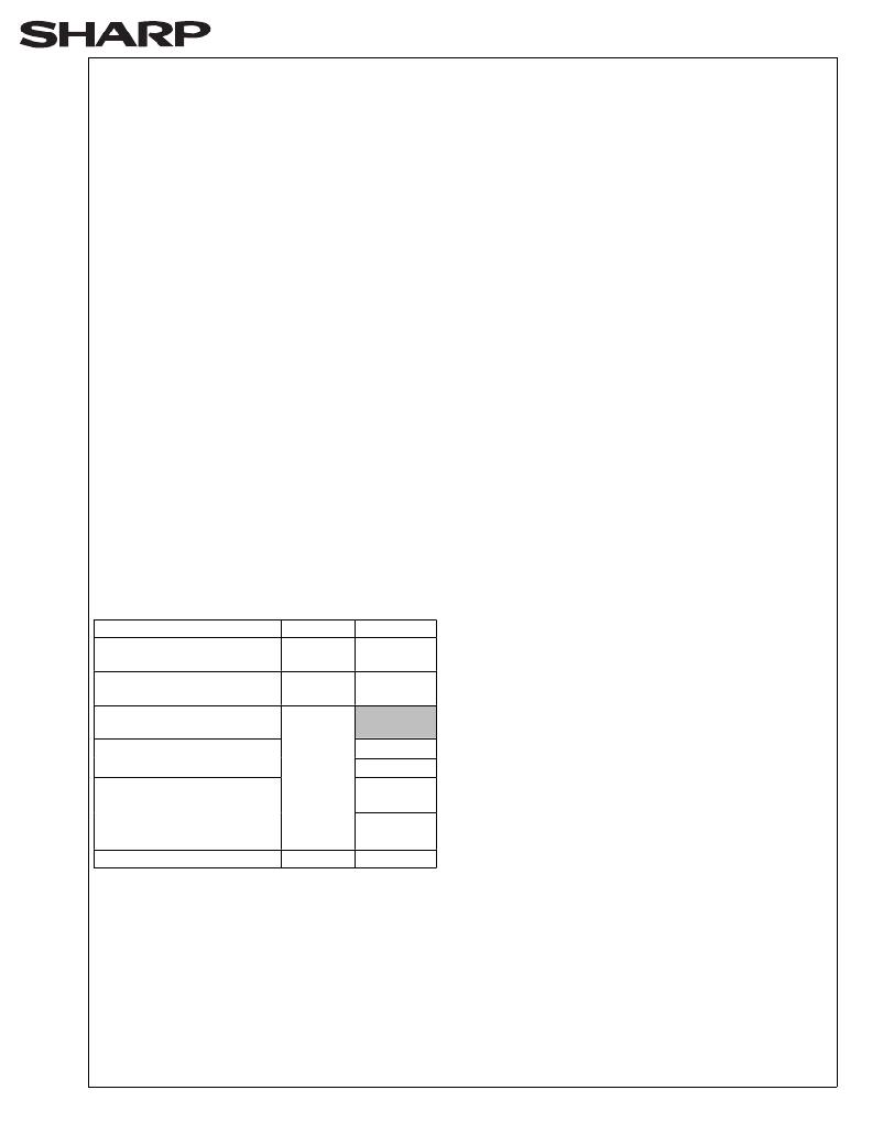
�Table� 5.� Identifier� Codes�
�4.3� Read� Status� Register� Command�
�The� status� register� may� be� read� to� determine� when� a�
�block� erase,� full� chip� erase,� (multi)� word/byte� write� or�
�block� lock-bit� configuration� is� complete� and� whether�
�the� operation� completed� successfully(see� Table� 14).�
�It� may� be� read� at� any� time� by� writing� the� Read� Status�
�Register� command.� After� writing� this� command,� all�
�subsequent� read� operations� output� data� from� the�
�status� register� until� another� valid� command� is� written.�
�The� status� register� contents� are� latched� on� the� falling�
�edge� of� OE#� or� CE#(Either� CE� 0� #� or� CE� 1� #),�
�whichever� occurs.� OE#� or� CE#(Either� CE� 0� #� or� CE� 1� #)�
�must� toggle� to� V� IH� before� further� reads� to� update� the�
�status� register� latch.� The� Read� Status� Register�
�command� functions� independently� of� the� V� PP� voltage.�
�RP#� must� be� V� IH� .�
�The� extended� status� register� may� be� read� to�
�determine� multi� word/byte� write� availability(see� Table�
�14.1).� The� extended� status� register� may� be� read� at�
�any� time� by� writing� the� Multi� Word/Byte� Write�
�command.� After� writing� this� command,� all� subsequent�
�read� operations� output� data� from� the� extended� status�
�register,� until� another� valid� command� is� written.� Multi�
�Word/Byte� Write� command� must� be� re-issued� to�
�update� the� extended� status� register� latch.�
�4.4� Clear� Status� Register� Command�
�Status� register� bits� SR.5,� SR.4,� SR.3� and� SR.1� are�
�set� to� "1"s� by� the� WSM� and� can� only� be� reset� by� the�
�Code�
�Manufacture� Code�
�Device� Code�
�Address�
�00000�
�00001�
�00002�
�00003�
�Data�
�B0�
�D0�
�Clear� Status� Register� command.� These� bits� indicate�
�various� failure� conditions� (see� Table� 14).� By� allowing�
�system� software� to� reset� these� bits,� several�
�operations� (such� as� cumulatively� erasing� or� locking�
�multiple� blocks� or� writing� several� bytes� in� sequence)�
�X0004�
�Block� Status� Code�
�?� Block� is� Unlocked�
�?� Block� is� Locked�
�?� Last� erase� operation�
�completed� successfully�
�?� Last� erase� operation� did�
�not� completed� successfully�
�?� Reserved� for� Future� Use�
�(1)�
�X0005� (1)�
�DQ� 0� =0�
�DQ� 0� =1�
�DQ� 1� =0�
�DQ� 1� =1�
�DQ� 2-7�
�may� be� performed.� The� status� register� may� be� polled�
�to� determine� if� an� error� occurs� during� the� sequence.�
�To� clear� the� status� register,� the� Clear� Status� Register�
�command� (50H)� is� written.� It� functions� independently�
�of� the� applied� V� PP� Voltage.� RP#� must� be� V� IH� .� This�
�command� is� not� functional� during� block� erase,� full�
�chip� erase,� (multi)� word/byte� write� block� lock-bit�
�configuration,� block� erase� suspend� or� (multi)�
�word/byte� write� suspend� modes.�
�NOTE:�
�1.� X� selects� the� specific� block� status� code� to� be�
�read.� See� Figure� 4� for� the� device� identifier� code�
�memory� map.�
�Rev.� 2.0�
�发布紧急采购,3分钟左右您将得到回复。
相关PDF资料
LH28F320S3HNS-ZM
IC FLASH 32MBIT 110NS 56SSOP
LH28F320SKTD-ZR
IC FLASH 32MBIT 70NS 48TSOP
LHF00L28
IC FLASH 16MBIT 70NS 48TSOP
LPM409 CHASSIS
STNRD 4SLOT CHASSIS W/INPUT LEAD
LS15RB1201J04
POE SPLITTER 10.8W 12V @0.9A
LT1932ES6#TRMPBF
IC LED DRIVR WHITE BCKLGT TSOT-6
LT1937ES5#TRMPBF
IC LED DRIVR WHITE BCKLGT TSOT-5
LT3003EMSE#TRPBF
IC LED DRIVER BALLASTER 10-MSOP
相关代理商/技术参数
LH28F160S5HR-L10
制造商:未知厂家 制造商全称:未知厂家 功能描述:x8/x16 Flash EEPROM
LH28F160S5HR-L70
制造商:未知厂家 制造商全称:未知厂家 功能描述:x8/x16 Flash EEPROM
LH28F160S5HT-L10
制造商:未知厂家 制造商全称:未知厂家 功能描述:x8/x16 Flash EEPROM
LH28F160S5HT-L70
功能描述:IC FLASH 16MBIT 70NS 56TSOP RoHS:否 类别:集成电路 (IC) >> 存储器 系列:- 标准包装:96 系列:- 格式 - 存储器:闪存 存储器类型:FLASH 存储容量:16M(2M x 8,1M x 16) 速度:70ns 接口:并联 电源电压:2.65 V ~ 3.6 V 工作温度:-40°C ~ 85°C 封装/外壳:48-TFSOP(0.724",18.40mm 宽) 供应商设备封装:48-TSOP 包装:托盘
LH28F160S5HT-L70T/R
制造商:Sharp Microelectronics 功能描述:YSM SMART,64K BLOCK, 70NS
LH28F160S5HT-TW
功能描述:IC FLASH 16MBIT 70NS 56TSOP RoHS:是 类别:集成电路 (IC) >> 存储器 系列:- 标准包装:1 系列:- 格式 - 存储器:RAM 存储器类型:SDRAM 存储容量:256M(8Mx32) 速度:143MHz 接口:并联 电源电压:3 V ~ 3.6 V 工作温度:-40°C ~ 85°C 封装/外壳:90-VFBGA 供应商设备封装:90-VFBGA(8x13) 包装:托盘 其它名称:Q2841869
LH28F160S5-L
制造商:SHARP 制造商全称:Sharp Electrionic Components 功能描述:16 M-bit (2 MB x 8/1 MB x 16) Smart 5 Flash Memories (Fast Programming)
LH28F160S5-L10
制造商:SHARP 制造商全称:Sharp Electrionic Components 功能描述:16-MBIT(2MBx8/MBx16)Smart 5 Flash MEMORY